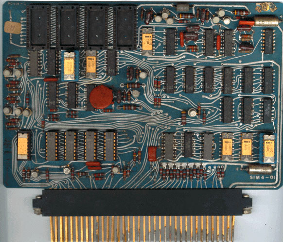
world's first microprocessor (16 pin DIP)
                         Intel

            4       000       000         4
           44      0   0     0   0       44
          4 4     0   0 0   0   0 0     4 4
         4  4     0  0  0   0  0  0    4  4
        4444444   0 0   0   0 0   0   4444444
            4      0   0     0   0        4
            4       000       000         4
pinouts:
                  _______    _______
                _|       \__/       |_
       <--> D0 |_|1               16|_| RAM0 -->
                _|                  |_
       <--> D1 |_|2               15|_| RAM1 -->
                _|                  |_
       <--> D2 |_|3               14|_| RAM2 -->
                _|                  |_
       <--> D3 |_|4               13|_| RAM3 -->
                _|       4004       |_
     (+5v) Vss |_|5               12|_| Vdd (-10v)
                _|                  |_
      --> CLK1 |_|6               11|_| ROM  -->
                _|                  |_
      --> CLK2 |_|7               10|_| TST <--
                _|                  |_
      <-- SYNC |_|8                9|_| RST <--
                 |__________________|
instruction set:
+----------+--+--+-+-------------------------------------------+
|Mnemonic  |W1|W2|T|Description                                |
+----------+--+--+-+-------------------------------------------+
|NOP       |00|  |E|No Operation                               |
|JCM c,aa  |1c|aa|G|Jumps to ROM address aa depending on c     |
|FIM Rm,dd |2s|dd|I|Fetch Immediate (Mov dd to reg pair s)     |
|SRC Rm    |2t|  |C|Send Register Control  (*1)                |
|FIN Rm    |3s|  |B|Fetch Indirect(Mov ROM at @R0R1 to s)      |
|JIN Rm    |3t|  |C|Jump Indirect (Jump to @t)                 |
|JUN aaa   |4a|aa|F|Jump Unconditional to ROM address aaa      |
|JMS aaa   |5a|aa|F|Jump to Subroutine at ROM address aaa      |
|INC Rn    |6r|  |A|Increment register r                       |
|ISZ Rn aa |7r|aa|H|Increment register r jump to aa on Zero    |
|ADD Rn    |8r|  |A|Add register r to accumulator with carry   |
|SUB Rn    |9r|  |A|Subtract r to accumulator with borrow      |
|LD  Rn    |Ar|  |A|Load accumulator with contents of r        |
|XCH Rn    |Br|  |A|Exchange contents of r and accumulator     |
|BBL d     |Cd|  |D|Branch back (in stack) load imm d to accum |
|LDM d     |Dd|  |D|Load imm to accumulator                    |
|WRM       |E0|  |E|Write contents of accumulator to RAM       |
|WMP       |E1|  |E|Write contents of accum to RAM output port |
|WRR       |E2|  |E|Write contents of accum to ROM I/O lines   |
|WPM       |E3|  |E|Write accum to selected half-byte (*2)     |
|WR0       |E4|  |E|Write selected RAM status character 0 (*1) |
|WR1       |E5|  |E|Write RAM status char1 to accum (*1)       |
|WR2       |E6|  |E|Write RAM status char2 to accum (*1)       |
|WR3       |E7|  |E|Write RAM status char3 to accum (*1)       |
|SBM       |E8|  |E|Subtract selected RAM from accum (*1)      |
|RDM       |E9|  |E|mov selected RAM to the accum (*1)         |
|RDR       |EA|  |E|mov contents of ROM I/O lines to accum(*1) |
|ADM       |EB|  |E|Add selected RAM to accum with carry (*1)  |
|AD0       |EC|  |E|Read selected RAM status character 0 (*1)  |
|AD1       |ED|  |E|Read RAM status char1 from accum (*1)      |
|AD2       |EE|  |E|Read RAM status char2 from accum (*1)      |
|AD3       |EF|  |E|Read RAM status char3 from accum (*1)      |
|CLB       |F0|  |E|Clear Both (Accumulator and Carry)         |
|CLC       |F1|  |E|Clear Carry                                |
|IAC       |F2|  |E|Increment Accumulator                      |
|CMC       |F3|  |E|Complement Carry                           |
|CMA       |F4|  |E|Complement Accumulator                     |
|RAL       |F5|  |E|Rotate Left Accumulator and Carry          |
|RAR       |F6|  |E|Rotate Right Accumulator and Carry         |
|TCC       |F7|  |E|Transfer Carry to Accumulator then Clear   |
|DAC       |F8|  |E|Decrement Accumulator                      |
|TCS       |F9|  |E|Transfer Carry subtract then Clear         |
|STC       |FA|  |E|Set Carry                                  |
|DAA       |FB|  |E|Decimal Adjust Accumulator                 |
|KBP       |FC|  |E|Keyboard Proccess (*3)                     |
|DCL       |FD|  |E|Designate command line                     |
+----------+--+--+-+-------------------------------------------+

+--------------------------------------------------------------+
| Instruction Format                                           |
+---------+------+----+----------------------------------------+
|  Word1  |Word2 |Type|            Notes                       |
+---------+------+----+----------------------------------------+
| ----rrrr       |A   |rrrr=R0/R1/.../RE/RF (4 bits)           |
| ----rrr0       |B   |rrr=R0R1/.../RERF (3 bits)              |
| ----rrr1       |C   |rrr=even numbered Reg Pairs (see above) |
| ----dddd       |D   |dddd=4 bits of immediate data           |
| --------       |E   |                                        |
| ----xxxx XX    |F   |aaaa=upper 4 bit address XX=Lower 8 addr|
| ----cccc XX    |G   |cccc=condition reg. XX=Lower 8 bit addr |
| ----rrrr XX    |H   |rrrr=R0/R1/.../RE/RF XX=Lower 8 bit addr|
| ----rrr0 DD    |I   |DD=Data                                 |
+----------------+----+----------------------------------------+

+------------------+-------------------------------------------+
|Hex Variable      |Description                                |
+------------------+-------------------------------------------+
|r                 |R0/R1/R2/R3/.../RD/RE/RF                   |
|s                 |Reg Pairs R0R1/.../RERF followed by bin 0  |
|t                 |Reg Pairs R0R1/.../RERF followed by bin 1  |
|a                 |Upper Address A11,A10,A9,A8                |
|aa                |Middle and Lower Address A7,A6,..,A1,A0    |
|d                 |Four bits of immediate data                |
|dd                |Eight bits of immediate data               |
|c                 |condition reg. c1c2c3c4 (*4)               |
+------------------+-------------------------------------------+

+------------------+-------------------------------------------+
|Mnemonic Variable |Description                                |
+------------------+-------------------------------------------+
|Rn                |R0/R1/R2/R3/.../RD/RE/RF (4 bits)          |
|Rm                |Reg pairs R0R1/R2R3/R4R5/.../RERF (3 bits) |
|dd                |8 bits of immediate data                   |
|d                 |4 bits of immediate data                   |
|aa                |8 bit address                              |
|aaa               |12 bit address                             |
|c                 |condition reg. c1c2c3c4 (4)
+------------------+-------------------------------------------+

(*1) SRC selects the address (And RAM banks) for the I/O instructions
     (All instructions with an "E" OPR)

(*2) For use with 4008/4009

(*3) Converts contents of the accumulator from a one out
     of four code to a binary code

(*4) c1:Invert Jump Condition (if c1==1)
     c2:Accumulator Equals Zero Condition
     c3:Carry Equals One Condition
     c4:Test Signal (TST - Pin 10) equals Zero Condition
- 3mm by 4mm die (1/8in by 1/6in) chip
- 10 micron tech.
- 2300 transistors
- initially US $200
- can address 640 bytes
- 500 kHz to 740 kHz
- typically 60000 instructions/sec.
- 50 8 bit instuctions (originally only had 46 instructions)
world's first microcomputer: